
In this article we are going to continue learning about the I2C bus and how it can work for us. If you have not already, please read and understand the first I2C article before continuing.
First of all, there are some limitations of I2C to take into account when designing your projects. One of these is the physical length of the SDA and SCL lines. If all your devices are on the same PCB, then there is nothing to worry about, however if your I2C bus is longer than around one metre, it is recommended that you use an I2C bus extender IC.
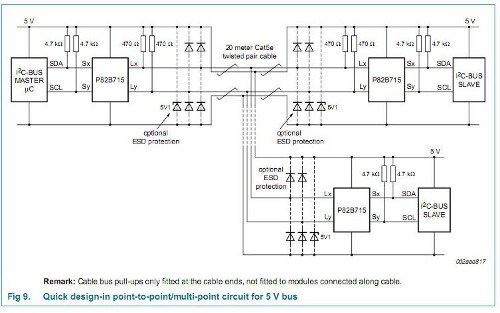
These ICs reduce electrical noise over the extended-length bus runs and buffer the I2C signals to reduce signal degradation and chance of errors in the data. An example of such an IC is the NXP P82B715 (data sheet).
Using a pair of these ICs, you can have cable runs of 20 to 30 metres, using shielded twisted-pair cable. Below is a good example of this, from the aforementioned NXP data sheet:
Several applications come to mind with an extended I2C bus, for example remote temperature monitoring using the the ST Microelectronics CN75 temperature sensor from part one; or controlling several I/O ports using an I2C expander without the expense or worry of using a wireless system. Speaking of which, let’s do that now…
A very useful and inexpensive part is the PCF8574 I/O expander (data sheet.pdf). This gives us another eight outputs, in a very similar method to the 74HC595; or can be used as eight extra inputs. In fact, if you were to use more than one 74HC595 this IC might be preferable, as you can individually address each chip instead of having to readdress every IC in line as you would with shift registers. So how do we do this? First, let’s consult the pinout:
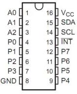

There should not be any surprises for you there. A2~A0 are used to select the last three bits of the device address, P0~P7 are the I/O pins, and INT is an interrupt output which we will not use. To address the PCF8574 we need two things, the device address, and a byte of data which represents the required output pin state. Huh? Consider:

So if we set pins A0 to A2 to GND, our device address in binary will be 0100000, or 0x20 in hexadecimal. And the same again to set the output pins, for example to turn them all on we send binary 0 in hexadecimal which is 0; or to have the first four on and the second four off, use 00001111 which is Ox0F. Hopefully you noticed that those last two values seemed backwards – why would we send a zero to turn all the pins on?
The reason is that the PCF8574 is a current sink. This means that current runs from +5v, through into the I/O pins. For example, an LED would have the anode on the +5V, and the cathode connected to an I/O pin. Normally (for example with a 74HC595) current would run from the IC, through the resistor, LED and then to earth. That is a current source. Consider the following quick diagram:

In the example above, please note that the PCF8574N can take care of current limitation with LEDs, whereas the 74HC595 needs a current-limiting resistor to protect the LED.
Luckily this IC can handle higher volumes of current, so a resistor will not be required. It sounds a bit odd, but like anything is easy once you spend a few moments looking into it. So now let’s use three PCF8574s to control 24 LEDs. To recreate this masterpiece of blinkiness you will need:
- Arduino Uno or compatible board
- A large solderless breadboard
- Three PCF8574 I/O extenders
- Eight each of red, green and yellow (or your choice) LEDs, each with a current draw of no more than 20mA
- Two 4.7 kilo ohm resistors
- Hook-up wires
- Three 0.1 uF ceramic capacitors
Here is the schematic:

…and the example sketch. Note that the device addresses in the sketch match the schematic above. If for some reason you are wiring your PCF8574s differently, you will need to recalculate your device addresses:
#include "Wire.h"
#define redchip 0x20 // device addresses for PCF8547Ns on each LED colour bank
#define yellowchip 0x22 // addresses in this example match the published schematic in the tutorial
#define greenchip 0x21 // you will need to change addresses if you vary from the schematic
int dd=20; // used for delay timing

void setup()
{
 Wire.begin();
 allOff(); // the PCF8574N defaults to high, so this functions turns all outputs off
}

// remember that the IC "sinks" current, that is current runs fro +5v through the LED and then to I/O pin
// this means that 'high' = off, 'low' = on.

void testfunc()
{
 Wire.beginTransmission(redchip);
 Wire.write(0);
 Wire.endTransmission();
 delay(dd+50);
 Wire.beginTransmission(redchip);
 Wire.write(255);
 Wire.endTransmission();
 delay(dd+50);
 Wire.beginTransmission(yellowchip);
 Wire.write(0);
 Wire.endTransmission();
 delay(dd+50);
 Wire.beginTransmission(yellowchip);
 Wire.write(255);
 Wire.endTransmission();
 delay(dd+50);
 Wire.beginTransmission(greenchip);
 Wire.write(0);
 Wire.endTransmission();
 delay(dd+50);
 Wire.beginTransmission(greenchip);
 Wire.write(255);
 Wire.endTransmission();
 delay(dd+50);
}

void testfunc2()
{
 for (int y=1; y<256; y*=2)
 {
 Wire.beginTransmission(redchip);
 Wire.write(255-y); // we need the inverse, that is high = off
 Wire.endTransmission();
 delay(dd);
 Wire.beginTransmission(redchip);
 Wire.write(255);
 Wire.endTransmission();
 delay(dd);
 }

 for (int y=1; y<256; y*=2)
 {
 Wire.beginTransmission(yellowchip);
 Wire.write(255-y);
 Wire.endTransmission();
 delay(dd);
 Wire.beginTransmission(yellowchip);
 Wire.write(255);
 Wire.endTransmission();
 delay(dd);
 }
 for (int y=1; y<256; y*=2)
 {
 Wire.beginTransmission(greenchip);
 Wire.write(255-y);
 Wire.endTransmission();
 delay(dd);
 Wire.beginTransmission(greenchip);
 Wire.write(255);
 Wire.endTransmission();
 delay(dd);
 }
}

void testfunc3()
{
 Wire.beginTransmission(redchip);
 Wire.write(0);
 Wire.endTransmission();
 Wire.beginTransmission(yellowchip);
 Wire.write(0);
 Wire.endTransmission();
 Wire.beginTransmission(greenchip);
 Wire.write(0);
 Wire.endTransmission();
 delay(dd+50);
 allOff();
 delay(dd+50);
}

void allOff()
{
 Wire.beginTransmission(redchip);
 Wire.write(255);
 Wire.endTransmission();
 Wire.beginTransmission(yellowchip);
 Wire.write(255);
 Wire.endTransmission();
 Wire.beginTransmission(greenchip);
 Wire.write(255);
 Wire.endTransmission();
}

void loop()
{
 for (int z=0; z<10; z++)
 {
 testfunc();
 }
 for (int z=0; z<10; z++)
 {
 testfunc2();
 }
 for (int z=0; z<10; z++)
 {
 testfunc3();
 }
}
And finally our demonstration video:
That was a good example of controlling many outputs with our humble I2C bus. You could literally control hundreds of outputs if necessary – a quite inexpensive way of doing so. Don’t forget to take into account the total current draw of any extended circuits if you are powering from your Arduino boards.
Using I2C EEPROMS
The next devices to examine on our I2C bus ride are EEPROMs – Electrically Erasable Programmable Read-Only Memory. These are memory chips that can store data without requiring power to retain memory. Why would we want to use these?
Sometimes you might need to store a lot of reference data for use in calculations during a sketch, such as a mathematical table; or perhaps numerical representations of maps or location data; or create your own interpreter within a sketch that takes instruction from data stored in an array.
In other words, an EEPROM can be used to store data of a more permanent use, ideal for when your main microcontroller doesn’t haven enough memory for you to store the data in the program code. However, EEPROMs are not really designed for random-access or constant read/write operations – they have a finite lifespan. But their use is quite simple, so we can take advantage of them.
EEPROMS, like anything else come in many shapes and sizes. The model we will examine today is the Microchip 24LC256 (data sheet.pdf). It can hold 256 kilobits of data (that’s 32 kilobytes) and is quite inexpensive. This model also has selectable device addresses using three pins, so we can use up to eight at once on the same bus. An example:

The pinouts are very simple:
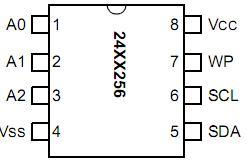
Pin 7 is “write protect” – set this low for read/write or high for read only. You could also control this in software if necessary. Once again we need to create a slave I2C device address using pins 1, 2 and 3 – these correlate to A2, A1 and A0 in the following table:
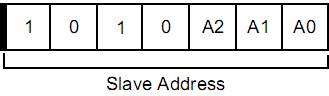
So if you were just using one 24LC256, the easiest solution would be to set A0~A2 to GND – which makes your slave address 1010000 or 0x50 in hexadecimal. There are several things to understand when it comes to reading and writing our bytes of data.
As this IC has 32 kilobytes of storage, we need to be able to reference each byte in order to read or write to it. There is a slight catch in that you need more than one byte to reference 32767 (as in binary 32767 is 11111111 0100100 [16 bits]).
So when it comes time to send read and write requests, we need to send two bytes down the bus – one representing the higher end of the address (the first 8 bits from left to right), and the next one representing the lower end of the address (the final 8 bits from left to right) – see figure 6.1 on page 9 of the data sheet.
An example – we need to reference byte number 25000. In binary, 25000 is 0110000110101000. So we split that up into 01100001 and 10101000, then covert the binary values to numerical bytes with which to send using the Wire.send(). Thankfully there are two operators to help us with this.
This first is >>, known as bitshift right. This will take the higher end of the byte and drop off the lower end, leaving us with the first 8 bits. To isolate the lower end of the address, we use another operator &, known as bitwise and. This unassuming character, when used with 0XFF can separate the lower bits for us. This may seem odd, but will work in the examples below.
Writing data to the 24LC256
Writing data is quite easy. But first remember that a byte of data is 11111111 in binary, or 255 in decimal. First we wake up the I2C bus with:
Wire.beginTransmission(0x50); // if pins A0~A2 are set to GND
then send down some data. The first data are the two bytes representing the address (25000) of the byte (12) we want to write to the memory.
Wire.write(25000 >> 8);  // send the left-hand side of the address down
Wire.write(25000 & 0xFF); // send the right-hand side of the address down
And finally, we send the byte of data to store at address 25000, then finish the connection:
Wire.write(12);
Wire.endTransmission();
There we have it. Now for getting it back…
Reading data from the 24LC256
Reading is quite similar. First we need to start things up and move the pointer to the data we want to read:
Wire.beginTransmission(0x50); // if pins A0~A2 are set to GND
Wire.write(25000 >> 8);  // send the left-hand side of the address down
Wire.write(25000 & 0xFF); // send the right-hand side of the address down
Wire.endTransmission();
Then, ask for the byte(s) of data starting at the current address:
Wire.beginTransmission(0x50); // if pins A0~A2 are set to GND
Wire.requestFrom(0x50,1);
Wire.read(incomingbyte);
In this example, incomingbyte is a byte variable used to store the data we retrieved from the IC. Now we have the theory, let’s put it into practice with the test circuit below, which contains two 24LC256 EEPROMs. To recreate this you will need:
- Arduino Uno or compatible board
- A large solderless breadboard
- Two Microchip 24LC256 EEPROMs (you can use 24LC512s as well)
- Two 4.7 kilo ohm resistors
- Hook-up wires
- Two 0.1 uF ceramic capacitors
Here is the schematic:

…and the example sketch. Note that the device addresses in the sketch match the schematic above. If for some reason you are wiring your 24LC256s differently, you will need to recalculate your device addresses. To save time with future coding, we have our own functions for reading and writing bytes to the EEPROM – readData() and writeData(). Consider the sketch for our example:
#include "Wire.h"  // for I2C
#define chip1 0x50 // device address for left-hand chip on our breadboard
#define chip2 0x51 // and the right

// always have your values in variables
unsigned int pointer = 69; // we need this to be unsigned, as you may have an address > 32767
byte d=0; // example variable to handle data going in and out of EERPROMS

void setup()
{
  Serial.begin(9600); // for screen output
  Wire.begin(); // wake up, I2C!
}

void writeData(int device, unsigned int add, byte data)
// writes a byte of data 'data' to the chip at I2C address 'device', in memory location 'add'
{
  Wire.beginTransmission(device);
  Wire.write((int)(add >> 8)); // left-part of pointer address
  Wire.write((int)(add & 0xFF)); // and the right
  Wire.write(data);
  Wire.endTransmission();
  delay(10);
}

byte readData(int device, unsigned int add)
// reads a byte of data from memory location 'add' in chip at I2C address 'device'
{
  byte result; // returned value
  Wire.beginTransmission(device); // these three lines set the pointer position in the EEPROM
  Wire.write((int)(add >> 8)); // left-part of pointer address
  Wire.write((int)(add & 0xFF)); // and the right
  Wire.endTransmission();
  Wire.requestFrom(device,1); // now get the byte of data...
  result = Wire.read();
  return result; // and return it as a result of the function readData
}

void loop()
{
  Serial.println("Writing data...");
  for (int a=0; a<20; a++)
  {
    writeData(chip1,a,a);
    writeData(chip2,a,a); // looks like a tiny EEPROM RAID solution!
  }
  Serial.println("Reading data...");
  for (int a=0; a<20; a++)
  {
    Serial.print("chip1 pointer ");
    Serial.print(a);
    Serial.print(" holds ");
    d=readData(chip1,a);
    Serial.println(d, DEC);
  }
  for (int a=0; a<20; a++)
  {
    Serial.print("chip2 pointer ");
    Serial.print(a);
    Serial.print(" holds ");
    d=readData(chip2,a);
    Serial.println(d, DEC);
  }
}
And the output from the example sketch:

Although the sketch in itself was simple, you now have the functions to read and write byte data to EEPROMS. Now it is up to your imagination to take use of the extra memory.
I hope you enjoyed reading about the I2C bus. If you find this sort of thing interesting, please consider ordering one or more of my books from amazon.
To keep up to date with new posts at tronixstuff.com, please subscribe to the mailing list in the box on the right, or follow us on x – @tronixstuff.
And as always, have fun and make something.


You must be logged in to post a comment.