Tag Archives: bus

Tutorial: Arduino and the SPI bus

This is the first of two chapters in which we are going to start investigating the SPI data bus, and how we can control devices using it with our Arduino systems.

The SPI bus may seem to be a complex interface to master, however with some brief study of this explanation and practical examples you will soon become a bus master! To do this we will learn the necessary theory, and then apply it by controlling a variety of devices. In this tutorial things will be kept as simple as possible.

But first of all, what is it? And some theory…

SPI is an acronym for “Serial Peripheral Interface”. It is a synchronous serial data bus – data can travel in both directions at the same time, as opposed to (for example) the I2C bus that cannot do so. To allow synchronous data transmission, the SPI bus uses four wires. They are called:

  • MOSI – Master-out, Slave-in. This line carries data from our Arduino to the SPI-controlled device(s);
  • MISO – Master-in, Slave out. This line carries data from the SPI-controlled device(s) back to the Arduino;
  • SS – Slave-select. This line tells the device on the bus we wish to communicate with it. Each SPI device needs a unique SS line back to the Arduino;
  • SCK – Serial clock.

Within these tutorials we consider the Arduino board to be the master and the SPI devices to be slaves. On our Arduino Uno and compatible boards the pins used are:

  • SS – digital 10. You can use other digital pins, but 10 is generally the default as it is next to the other SPI pins;
  • MOSI – digital 11;
  • MISO – digital 12;
  • SCK – digital 13;

Arduino Mega users – MISO is 50, MOSI is 51, SCK is 52 and SS is usually 53. If you are using an Arduino Leonardo, the SPI pins are on the ICSP header pins. See here for more information. You can control one or more devices with the SPI bus. For example, for one device the wiring would be:

sspiss1

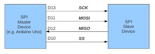
Data travels back and forth along the MOSI and MISO lines between our Arduino and the SPI device. This can only happen when the SS line is set to LOW. In other words, to communicate with a particular SPI device on the bus, we set the SS line to that device to LOW, then communicate with it, then set the line back to HIGH. If we have two or more SPI devices on the bus, the wiring would resemble the following:

sspiss2


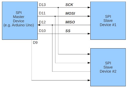
Notice how there are two SS lines – we need one for each SPI device on the bus. You can use any free digital output pin on your Arduino as an SS line. Just remember to have all SS lines high except for the line connected to the SPI device you wish to use at the time.

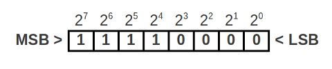
Data is sent to the SPI device in byte form. You should know by now that eight bits make one byte, therefore representing a binary number with a value of between zero and 255.

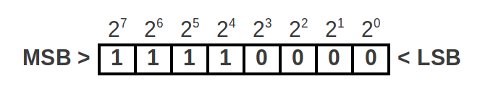
When communicating with our SPI devices, we need to know which way the device deals with the data – MSB or LSB first. MSB (most significant bit) is the left-hand side of the binary number, and LSB (least significant bit) is the right-hand side of the number. That is:

binnum

Apart from sending numerical values along the SPI bus, binary numbers can also represent commands. You can represent eight on/off settings using one byte of data, so a device’s parameters can be set by sending a byte of data. These parameters will vary with each device and should be illustrated in the particular device’s data sheet. For example, a digital potentiometer IC with six pots:

sdata1

This device requires two bytes of data. The ADDR byte tells the device which of six potentiometers to control (numbered 0 to 5), and the DATA byte is the value for the potentiometer (0~255). We can use integers to represent these two values. For example, to set potentiometer number two to 125, we would send 2 then 125 to the device.

How do we send data to SPI devices in our sketches?

First of all, we need to use the SPI library. It is included with the default Arduino IDE installation, so put the following at the start of your sketch:

#include "SPI.h"

Next, in void.setup() declare which pin(s) will be used for SS and set them as OUTPUT. For example,

pinMode(ss, OUTPUT);

where ss has previously been declared as an integer of value ten. Now, to activate the SPI bus:

SPI.begin();

and finally we need to tell the sketch which way to send data, MSB or LSB first by using

SPI.setBitOrder(MSBFIRST);

or

SPI.setBitOrder(LSBFIRST);

When it is time to send data down the SPI bus to our device, three things need to happen. First, set the digital pin with SS to low:

digitalWrite(SS, LOW);

Then send the data in bytes, one byte at a time using:

SPI.transfer(value);

Value can be an integer/byte between zero and 255. Finally, when finished sending data to your device, end the transmission by setting SS high:

digitalWrite(ss, HIGH);

Sending data is quite simple. Generally the most difficult part for people is interpreting the device data sheet to understand how commands and data need to be structured for transmission. But with some practice, these small hurdles can be overcome.

Now for some practical examples!

Time to get on the SPI bus and control some devices. By following the examples below, you should gain a practical understanding of how the SPI bus and devices can be used with our Arduino boards.

MCP4162 Example

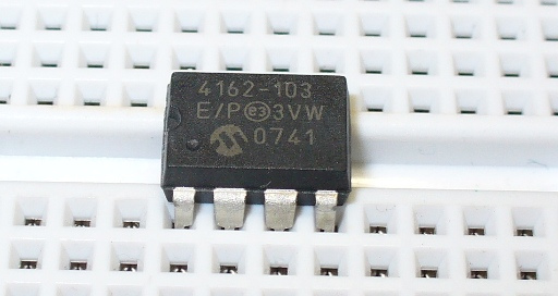
Our first example will use a simple yet interesting part – a digital potentiometer (we also used one in the I2C tutorial). This time we have a Microchip MCP4162-series 10k rheostat:

digipotss

Here is the data sheet for your perusal. To control it we need to send two bytes of data – the first byte is the control byte, and thankfully for this example it is always zero (as the address for the wiper value is 00h [see table 4-1 of the data sheet]).  The second byte is the the value to set the wiper, which controls the resistance. So to set the wiper we need to do three things in our sketch…

First, set the SS (slave select) line to low:

digitalWrite(10, LOW);

Then send the two byes of data:

SPI.transfer(0); // command byte
SPI.transfer(value); // wiper value

Finally set the SS line back to high:

digitalWrite(10, HIGH);

Easily done. Connection to our Arduino board is very simple – consider the MCP4162 pinout:

mcp4162pinout

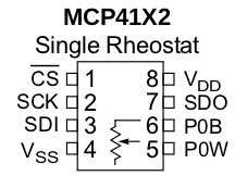
Vdd connects to 5V, Vss to GND, CS to digital 10, SCK to digital 13, SDI to digital 11 and SDO to digital 12. Now let’s run through the available values of the MCP4162 in the following sketch:

/*
 SPI bus demo using a Microchip MCP4162 digital potentiometer [http://bit.ly/iwDmnd]
 */

#include "SPI.h" // necessary library
int ss=10; // using digital pin 10 for SPI slave select
int del=200; // used for various delays

void setup()
{
  pinMode(ss, OUTPUT); // we use this for SS pin
  SPI.begin(); // wake up the SPI bus.
  SPI.setBitOrder(MSBFIRST);
  // our MCP4162 requires data to be sent MSB (most significant byte) first
}

void setValue(int value)
{
  digitalWrite(ss, LOW);
  SPI.transfer(0); // send command byte
  SPI.transfer(value); // send value (0~255)
  digitalWrite(ss, HIGH);
}

void loop()
{
  for (int a=0; a<256; a++)
  {
    setValue(a);
    delay(del);
  }
  for (int a=255; a>=0; --a)
  {
    setValue(a);
    delay(del);
  }
}

Now to see the results of the sketch. In the following video clip, a we run up through the resistance range and measure the rheostat value with a multimeter:

Before moving forward, if digital potentiometers are new for you, consider reading this short guide written by Microchip about the differences between mechanical and digital potentiometers.

Another example:

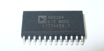
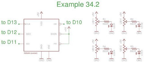
In this example, we will use the Analog Devices AD5204 four-channel digital potentiometer (data sheet.pdf). It contains four 10k ohm linear potentiometers, and each potentiometer is adjustable to one of 256 positions.

The settings are volatile, which means they are not remembered when the power is turned off. Therefore when power is applied the potentiometers are all pre set to the middle of the scale. Our example is the SOIC-24 surface mount example, however it is also manufactured in DIP format as well.

ad5204ss

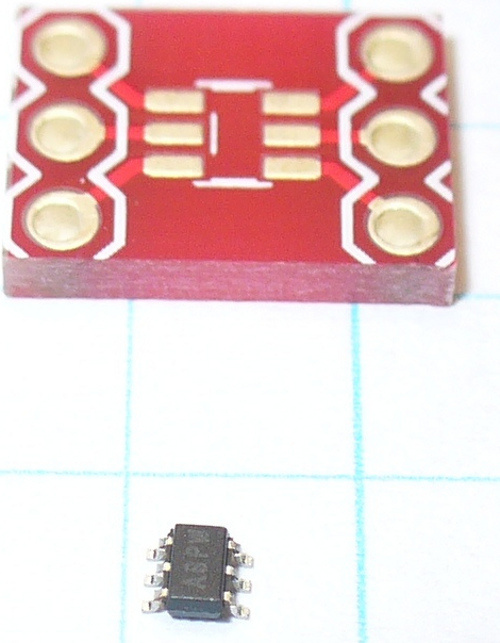
To make life easier it can be soldered onto a SOIC breakout board which converts it to a through-hole package:

ad5204boardss1

In this example, we will control the brightness of four LEDs. Wiring is very simple. Pinouts are in the data sheet.

ex34p2schematic1

And the sketch:

#include <SPI.h> // necessary library
int ss=10; // using digital pin 10 for SPI slave select
int del=5; // used for fading delay
void setup()
{
 pinMode(ss, OUTPUT); // we use this for SS pin
 SPI.begin(); // wake up the SPI bus. 
 SPI.setBitOrder(MSBFIRST); 
 // our AD5204 requires data to be sent MSB (most significant byte) first. See data sheet page 5
 allOff(); // we do this as pot memories are volatile
}
void allOff()
// sets all potentiometers to minimum value
{
 for (int z=0; z<4; z++)
 {
 setPot(z,0);
 }
}
void allOn()
// sets all potentiometers to maximum value
{
 for (int z=0; z<4; z++)
 {
 setPot(z,255);
 }
}
void setPot(int pot, int level)
// sets potentiometer 'pot' to level 'level'
{
 digitalWrite(ss, LOW);
 SPI.transfer(pot);
 SPI.transfer(level);
 digitalWrite(ss, HIGH);
}
void blinkAll(int count)
{
 for (int z=0; z
void indFade()
{
 for (int a=0; a<4; a++)
 {
 for (int l=0; l<255; l++)
 {
 setPot(a,l);
 delay(del);
 }
 for (int l=255; l>=0; --l)
 {
 setPot(a,l);
 delay(del);
 }
 }
}
void allFade(int count)
{
 for (int a=0; a<count; a++)="" {="" for="" (int="" l="0;" l<255;="" l++)="" setpot(0,l);="" setpot(1,l);="" setpot(2,l);="" setpot(3,l);="" delay(del);="" }="">=0; --l)
 {
 setPot(0,l);
 setPot(1,l);
 setPot(2,l); 
 setPot(3,l); 
 delay(del);
 }
 }
}
void loop()
{
 blinkAll(3);
 delay(1000);
 indFade();
 allFade(3);
}

The function allOff() and allOn() are used to set the potentiometers to minimum and maximum respectively. We use allOff() at the start of the sketch to turn the LEDs off. This is necessary as on power-up the wipers are generally set half-way.

Furthermore we use them in the blinkAll() function to … blink the LEDs. The function setPot() accepts a wiper number (0~3) and value to set that wiper (0~255). Finally the function indFade() does a nice job of fading each LED on and off in order – causing an effect very similar to pulse-width modulation.

Finally, here it is in action:

So there you have it – hopefully an easy to understand introduction to the world of the SPI bus and how to control the devices within. As always, now it is up to you and your imagination to find something to control or get up to other shenanigans. In the next SPI article we will look at reading and writing data via the SPI bus.

This post brought to you by pmdway.com – everything for makers and electronics enthusiasts, with free delivery worldwide.

To keep up to date with new posts at tronixstuff.com, please subscribe to the mailing list in the box on the right, or follow us on twitter @tronixstuff.

Tutorial: Arduino and the I2C bus – Part Two

In this article we are going to continue learning about the I2C bus and how it can work for us. If you have not already, please read and understand the first I2C article before continuing.

First of all, there are some limitations of I2C to take into account when designing your projects. One of these is the physical length of the SDA and SCL lines. If all your devices are on the same PCB, then there is nothing to worry about, however if your I2C bus is longer than around one metre, it is recommended that you use an I2C bus extender IC.

These ICs reduce electrical noise over the extended-length bus runs and buffer the I2C signals to reduce signal degradation and chance of errors in the data. An example of such an IC is the NXP P82B715 (data sheet).

Using a pair of these ICs, you can have cable runs of 20 to 30 metres, using shielded twisted-pair cable. Below is a good example of this, from the aforementioned NXP data sheet:

i2cbufferedss1

Several applications come to mind with an extended I2C bus, for example remote temperature monitoring using the the ST Microelectronics CN75 temperature sensor from part one; or controlling several I/O ports using an I2C expander without the expense or worry of using a wireless system. Speaking of which, let’s do that now…

A very useful and inexpensive part is the PCF8574 I/O expander (data sheet.pdf). This gives us another eight outputs, in a very similar method to the 74HC595; or can be used as eight extra inputs. In fact, if you were to use more than one 74HC595 this IC might be preferable, as you can individually address each chip instead of having to readdress every IC in line as you would with shift registers. So how do we do this? First, let’s consult the pinout:

pcf8574n_pinout

There should not be any surprises for you there. A2~A0 are used to select the last three bits of the device address, P0~P7 are the I/O pins, and INT is an interrupt output which we will not use. To address the PCF8574 we need two things, the device address, and a byte of data which represents the required output pin state. Huh? Consider:

pcf8574intdef1

So if we set pins A0 to A2 to GND, our device address in binary will be 0100000, or 0x20 in hexadecimal. And the same again to set the output pins, for example to turn them all on we send binary 0 in hexadecimal which is 0; or to have the first four on and the second four off, use 00001111 which is Ox0F. Hopefully you noticed that those last two values seemed backwards – why would we send a zero to turn all the pins on?

The reason is that the PCF8574 is a current sink. This means that current runs from +5v, through into the I/O pins. For example, an LED would have the anode on the +5V, and the cathode connected to an I/O pin. Normally (for example with a 74HC595) current would run from the IC, through the resistor, LED and then to earth. That is a current source. Consider the following quick diagram:

sinksource11

In the example above, please note that the PCF8574N can take care of current limitation with LEDs, whereas the 74HC595 needs a current-limiting resistor to protect the LED.

Luckily this IC can handle higher volumes of current, so a resistor will not be required. It sounds a bit odd, but like anything is easy once you spend a few moments looking into it. So now let’s use three PCF8574s to control 24 LEDs. To recreate this masterpiece of blinkiness you will need:

Here is the schematic:

exam21p1schemss1

…and the example sketch. Note that the device addresses in the sketch match the schematic above. If for some reason you are wiring your PCF8574s differently, you will need to recalculate your device addresses:

#include "Wire.h"
#define redchip 0x20 // device addresses for PCF8547Ns on each LED colour bank 
#define yellowchip 0x22 // addresses in this example match the published schematic in the tutorial
#define greenchip 0x21 // you will need to change addresses if you vary from the schematic
int dd=20; // used for delay timing

void setup()
{
 Wire.begin();
 allOff(); // the PCF8574N defaults to high, so this functions turns all outputs off
}

// remember that the IC "sinks" current, that is current runs fro +5v through the LED and then to I/O pin
// this means that 'high' = off, 'low' = on.

void testfunc()
{
 Wire.beginTransmission(redchip);
 Wire.write(0); 
 Wire.endTransmission();
 delay(dd+50);
 Wire.beginTransmission(redchip);
 Wire.write(255); 
 Wire.endTransmission();
 delay(dd+50);
 Wire.beginTransmission(yellowchip);
 Wire.write(0); 
 Wire.endTransmission();
 delay(dd+50);
 Wire.beginTransmission(yellowchip);
 Wire.write(255); 
 Wire.endTransmission();
 delay(dd+50);
 Wire.beginTransmission(greenchip);
 Wire.write(0); 
 Wire.endTransmission();
 delay(dd+50);
 Wire.beginTransmission(greenchip);
 Wire.write(255); 
 Wire.endTransmission();
 delay(dd+50);
}

void testfunc2()
{
 for (int y=1; y<256; y*=2)
 {
 Wire.beginTransmission(redchip);
 Wire.write(255-y); // we need the inverse, that is high = off
 Wire.endTransmission();
 delay(dd);
 Wire.beginTransmission(redchip);
 Wire.write(255); 
 Wire.endTransmission();
 delay(dd);
 }

 for (int y=1; y<256; y*=2)
 {
 Wire.beginTransmission(yellowchip);
 Wire.write(255-y); 
 Wire.endTransmission();
 delay(dd);
 Wire.beginTransmission(yellowchip);
 Wire.write(255); 
 Wire.endTransmission();
 delay(dd);
 }
 for (int y=1; y<256; y*=2)
 {
 Wire.beginTransmission(greenchip);
 Wire.write(255-y); 
 Wire.endTransmission();
 delay(dd);
 Wire.beginTransmission(greenchip);
 Wire.write(255); 
 Wire.endTransmission();
 delay(dd);
 }
}

void testfunc3()
{
 Wire.beginTransmission(redchip);
 Wire.write(0); 
 Wire.endTransmission();
 Wire.beginTransmission(yellowchip);
 Wire.write(0); 
 Wire.endTransmission();
 Wire.beginTransmission(greenchip);
 Wire.write(0); 
 Wire.endTransmission();
 delay(dd+50);
 allOff();
 delay(dd+50);
}

void allOff()
{
 Wire.beginTransmission(redchip);
 Wire.write(255); 
 Wire.endTransmission();
 Wire.beginTransmission(yellowchip);
 Wire.write(255); 
 Wire.endTransmission();
 Wire.beginTransmission(greenchip);
 Wire.write(255); 
 Wire.endTransmission();
}

void loop()
{
 for (int z=0; z<10; z++)
 {
 testfunc();
 }
 for (int z=0; z<10; z++)
 {
 testfunc2();
 }
 for (int z=0; z<10; z++)
 {
 testfunc3();
 }
}

 And finally our demonstration video:

That was a good example of controlling many outputs with our humble I2C bus. You could literally control hundreds of outputs if necessary – a quite inexpensive way of doing so. Don’t forget to take into account the total current draw of any extended circuits if you are powering from your Arduino boards.

Using I2C EEPROMS

The next devices to examine on our I2C bus ride are EEPROMs – Electrically Erasable Programmable Read-Only Memory. These are memory chips that can store data without requiring power to retain memory. Why would we want to use these?

Sometimes you might need to store a lot of reference data for use in calculations during a sketch, such as a mathematical table; or perhaps numerical representations of maps or location data; or create your own interpreter within a sketch that takes instruction from data stored in an array.

In other words, an EEPROM can be used to store data of a more permanent use, ideal for when your main microcontroller doesn’t haven enough memory for you to store the data in the program code. However, EEPROMs are not really designed for random-access or constant read/write operations – they have a finite lifespan. But their use is quite simple, so we can take advantage of them.

EEPROMS, like anything else come in many shapes and sizes. The model we will examine today is the Microchip 24LC256 (data sheet.pdf). It can hold 256 kilobits of data (that’s 32 kilobytes) and is quite inexpensive. This model also has selectable device addresses using three pins, so we can use up to eight at once on the same bus. An example:

24lc256bb1

The pinouts are very simple:

24lc256pinout

Pin 7 is “write protect” – set this low for read/write or high for read only. You could also control this in software if necessary. Once again we need to create a slave I2C device address using pins 1, 2 and 3 – these correlate to A2, A1 and A0 in the following table:

24lc256address

So if you were just using one 24LC256, the easiest solution would be to set A0~A2 to GND – which makes your slave address 1010000 or 0x50 in hexadecimal. There are several things to understand when it comes to reading and writing our bytes of data.

As this IC has 32 kilobytes of storage, we need to be able to reference each byte in order to read or write to it. There is a slight catch in that you need more than one byte to reference 32767 (as in binary 32767 is 11111111 0100100 [16 bits]).

So when it comes time to send read and write requests, we need to send two bytes down the bus – one representing the higher end of the address (the first 8 bits from left to right), and the next one representing the lower end of the address (the final 8 bits from left to right) – see figure 6.1 on page 9 of the data sheet.

An example – we need to reference byte number 25000. In binary, 25000 is 0110000110101000. So we split that up into 01100001 and 10101000, then covert the binary values to numerical bytes with which to send using the Wire.send(). Thankfully there are two operators to help us with this.

This first is >>, known as bitshift right. This will take the higher end of the byte and drop off the lower end, leaving us with the first 8 bits. To isolate the lower end of the address, we use another operator &, known as bitwise and. This unassuming character, when used with 0XFF can separate the lower bits for us. This may seem odd, but will work in the examples below.

Writing data to the 24LC256

Writing data is quite easy. But first remember that a byte of data is 11111111 in binary, or 255 in decimal. First we wake up the I2C bus with:

Wire.beginTransmission(0x50); // if pins A0~A2 are set to GND

then send down some data. The first data are the two bytes representing the address (25000) of the byte (12) we want to write to the memory.

Wire.write(25000 >> 8);  // send the left-hand side of the address down
Wire.write(25000 & 0xFF); // send the right-hand side of the address down

And finally, we send the byte of data to store at address 25000, then finish the connection:

Wire.write(12);
Wire.endTransmission();

There we have it. Now for getting it back…

Reading data from the 24LC256

Reading is quite similar. First we need to start things up and move the pointer to the data we want to read:

Wire.beginTransmission(0x50); // if pins A0~A2 are set to GND
Wire.write(25000 >> 8);  // send the left-hand side of the address down
Wire.write(25000 & 0xFF); // send the right-hand side of the address down
Wire.endTransmission();

Then, ask for the byte(s) of data starting at the current address:

Wire.beginTransmission(0x50); // if pins A0~A2 are set to GND
Wire.requestFrom(0x50,1);
Wire.read(incomingbyte);

In this example, incomingbyte is a byte variable used to store the data we retrieved from the IC. Now we have the theory, let’s put it into practice with the test circuit below, which contains two 24LC256 EEPROMs. To recreate this you will need:

Here is the schematic:

examp21p2schemss1

…and the example sketch. Note that the device addresses in the sketch match the schematic above. If for some reason you are wiring your 24LC256s differently, you will need to recalculate your device addresses. To save time with future coding, we have our own functions for reading and writing bytes to the EEPROM – readData() and writeData(). Consider the sketch for our example:

#include "Wire.h"  // for I2C
#define chip1 0x50 // device address for left-hand chip on our breadboard
#define chip2 0x51 // and the right

// always have your values in variables
unsigned int pointer = 69; // we need this to be unsigned, as you may have an address > 32767
byte d=0; // example variable to handle data going in and out of EERPROMS

void setup()
{
  Serial.begin(9600); // for screen output
  Wire.begin(); // wake up, I2C!
}

void writeData(int device, unsigned int add, byte data) 
// writes a byte of data 'data' to the chip at I2C address 'device', in memory location 'add'
{
  Wire.beginTransmission(device);
  Wire.write((int)(add >> 8)); // left-part of pointer address
  Wire.write((int)(add & 0xFF)); // and the right
  Wire.write(data);
  Wire.endTransmission();
  delay(10);
}

byte readData(int device, unsigned int add) 
// reads a byte of data from memory location 'add' in chip at I2C address 'device' 
{
  byte result; // returned value
  Wire.beginTransmission(device); // these three lines set the pointer position in the EEPROM
  Wire.write((int)(add >> 8)); // left-part of pointer address
  Wire.write((int)(add & 0xFF)); // and the right
  Wire.endTransmission();
  Wire.requestFrom(device,1); // now get the byte of data...
  result = Wire.read();
  return result; // and return it as a result of the function readData
}

void loop()
{
  Serial.println("Writing data...");
  for (int a=0; a<20; a++)
  {
    writeData(chip1,a,a);
    writeData(chip2,a,a); // looks like a tiny EEPROM RAID solution!
  }
  Serial.println("Reading data...");
  for (int a=0; a<20; a++)
  {
    Serial.print("chip1 pointer ");
    Serial.print(a);
    Serial.print(" holds ");
    d=readData(chip1,a);
    Serial.println(d, DEC);
  }
  for (int a=0; a<20; a++)
  {
    Serial.print("chip2 pointer ");
    Serial.print(a);
    Serial.print(" holds ");
    d=readData(chip2,a);
    Serial.println(d, DEC);
  } 
}

And the output from the example sketch:

example21p2result1

Although the sketch in itself was simple, you now have the functions to read and write byte data to EEPROMS. Now it is up to your imagination to take use of the extra memory.

This post brought to you by pmdway.com – everything for makers and electronics enthusiasts, with free delivery worldwide.

To keep up to date with new posts at tronixstuff.com, please subscribe to the mailing list in the box on the right, or follow us on twitter @tronixstuff.

Tutorial: Arduino and the I2C bus – Part One

In this first of several tutorials we are going to investigate the I2C data bus, and how we can control devices using it with our Arduino systems. The I2C bus can be a complex interface to master, so we will do my best to simplify it for you.

In this article we will learn the necessary theory, and then apply it by controlling a variety of devices. Furthermore it would be in your interest to have an understanding of the binary, binary-coded decimal and hexadecimal number systems.

But first of all, what is it?

I2C is an acronym for “Inter-Integrated Circuit”. In the late 1970s, Philips’ semiconductor division (now NXP) saw the need for simplifying and standardising the data lines that travel between various integrated circuits in their products.

Their solution was the I2C bus. This reduced the number of wires to two (SDA – data, and SCL – clock). Here is a nice introductory video from NXP:

Why would we want to use I2C devices?

As there are literally thousands of components that use the I2C interface. And our Arduino boards can control them all. There are many applications, such a real-time clocks, digital potentiometers, temperature sensors, digital compasses, memory chips, FM radio circuits, I/O expanders, LCD controllers, amplifiers, and so on.

And you can have more than one on the bus at any time, in fact the maximum number of I2C devices used at any one time is 112.

From a hardware perspective, the wiring is very easy. Those of you with an Arduino Uno or 100% compatible board, you will be using pins A4 for SDA (data) and A5 for SCL (clock):

CREATOR: gd-jpeg v1.0 (using IJG JPEG v80), quality = 90

If you are using an Arduino Mega, SDA is pin 20 and SCL is 21, so note that shields with I2C need to be specifically for the Mega. If you have another type of board, check your data sheet or try the Arduino team’s hardware website.

And finally, if you are using a bare DIP ATmega328-PU microcontroller, you will use pins 27 for SDA and 28 for SCL. The bus wiring is simple:

nxpi2cbussmall

If you are only using one I2C device, the pull-up resistors are (normally) not required, as the ATmega328 microcontroller in our Arduino has them built-in.  However if you are running a string of devices, use two 10 kilo ohm resistors.

Like anything, some testing on a breadboard or prototype circuit will determine their necessity. Sometimes you may see in a particular device’s data sheet the use of different value pull-up resistors – for example 4.7k ohm.

If so, heed that advice. The maximum length of an I2C bus is around one metre, and is a function of the capacitance of the bus. This distance can be extended with the use of a special IC, which we will examine during the next I2C chapter.

Each device can be connected to the bus in any order, and devices can be masters or slaves. In our Arduino situation, the board is the master and the devices on the I2C bus are the slaves.

We can write data to a device, or read data from a device. By now you should be thinking “how do we differentiate each device on the bus?”… Each device has a unique address. We use that address in the functions described later on to direct our read or write requests to the correct device.

It is possible to use two devices with identical addresses on an I2C bus, but that will be discussed in a later article.

As like most devices, we make use of an Arduino library, in this case <wire.h>. Then use the function Wire.begin(); inside of void setup() and we’re ready to go.

Sending data from our Arduino to the I2C devices requires two things: the unique device address (we need this in hexadecimal) and at least one byte of data to send. For example, the address of the part in example 20.1 (below) is 00101111 (binary) which is 0X2F in hexadecimal. Then we want to set the wiper value, which is a value between 0 and 127, or 0x00 and 0x7F in hexadecimal. So to set the wiper to zero, we would use the following three functions:

Wire.beginTransmission(0x2F);      // part address is 0x2F or 0101111

This sends the device address down the SDA (data) line of the bus. It travels along the bus, and “notifies” the matching device that it has some data coming…

Wire.write(0); // sends 0 down the bus

This sends the byte of data to the device – into the device register (or memory of sorts), which is waiting for it with open arms. Any other devices on the bus will ignore this.

Note that you can only perform one I2C operation at a time! Then when we have finished sending data to the device, we “end transmission”. This tells the device that we’re finished, and frees up the I2C bus for the next operation:

Wire.endTransmission();

Some devices may have more than one register, and require more bytes of data in each transmission. For example, the DS1307 real-time clock IC has eight registers to store timing data, each requiring eight bits of data (one byte):

ds1307registers1

However with the DS1307  – the entire lot need to be rewritten every time. So in this case we would use eight wire.send(); functions every time. Each device will interpret the byte of data sent to it, so you need the data sheet for your device to understand how to use it.

Receiving data from an I2C device into our Arduino requires two things: the unique device address (we need this in hexadecimal) and the number of bytes of data to accept from the device.

Receiving data at this point is a two stage process. If you review the table above from the DS1307 data sheet, note that there is eight registers, or bytes of data in there. The first thing we need to do is have the I2C device start reading from the first register, which is done by sending a zero to the device:

Wire.beginTransmission(device_address);
Wire.write(0);
Wire.endTransmission();

Now the I2C device will send data from the first register when requested. We now need to ask the device for the data, and how many bytes we want. For example, if a device held three bytes of data, we would ask for three, and store each byte in its own variable (for example, we have three variables of type byte: a, b, and c. The first function to execute is:

Wire.requestFrom(device_address, 3);

Which tells the device to send three bytes of data back to the Arduino. We then immediately follow this with:

*a = Wire.read();
*b = Wire.read();
*c = Wire.read();

We do not need to use Wire.endTransmission() when reading data. Now that the requested data is in their respective variables, you can treat them like any ordinary byte variable. For a more detailed explanation of the I2C bus, read this explanatory document by NXP. Now let’s use our I2C knowledge by controlling a range of devices…

The Microchip MCP4018T digital linear potentiometer. The value of this model is 10 kilo ohms. Inside this tiny, tiny SMD part is a resistor array consisting of 127 elements and a wiper that we control by sending a value of between 0 and 127 (in hexadecimal) down the I2C bus. This is a volatile digital potentiometer, it forgets the wiper position when the power is removed.

However naturally there is a compromise with using such a small part, it is only rated for 2.5 milliamps – but used in conjunction with op amps and so on. For more information, please consult the data sheet. As this is an SMD part, for breadboard prototyping purposes it needed to be mounted on a breakout board. Here it is in raw form:

mcp4018raw1

Above the IC is a breakout board. Consider that the graph paper is 5mm square! It is the incorrect size, but all I have. However soldering was bearable. Put a drop of solder on one pad of the breakout board, then hold the IC with tweezers in one hand, and reheat the solder with the other hand – then push the IC into place. A few more tiny blobs of solder over the remaining pins, and remove the excess with solder wick. Well … it worked for me:

mcp4018cooked1

Our example schematic is as follows:

mcp4018sch1

As you can see, the part is simple to use, your signal enters pin 6 and the result of the voltage division is found on pin 5. Please note that this is not a replacement for a typical mechanical potentiometer, we can’t just hook this up as a volume or motor-speed control! Again, please read the data sheet.

Control is very simple, we only need to send one byte of data down, the hexadecimal reference point for the wiper, e.g.:

Wire.beginTransmission(0x2F);      // part address is 0x2F or 0101111b
Wire.write(0x3F); //
Wire.endTransmission();

Here is a quick demonstration that moves the wiper across all points:

int dt = 2000; // used for delay duration
byte rval = 0x00; // used for value sent to potentiometer
#include "Wire.h"
#define pot_address 0x2F // each I2C object has a unique bus address, the MCP4018 is 0x2F or 0101111 in binary

void setup()
{
  Wire.begin();
  Serial.begin(9600); 
}

void potLoop()
// sends values of 0x00 to 0x7F to pot in order to change the resistance
// equates to 0~127
{
  for (rval=0; rval<128; rval++)
  {
    Wire.beginTransmission(pot_address);
    Wire.write(rval); // 
    Wire.endTransmission();
    Serial.print(" sent - ");
    Serial.println(rval, HEX);
    delay(dt);
  }
}

void loop()
{
  potLoop();
}

 and a video demonstration:

Now we will read some data from an I2C device. Our test subject is the ST Microelectronics CN75 temperature sensor. Again, we have another SMD component, but the CN75 is the next stage larger than the part from example 20.1. Thankfully this makes the soldering process much easier, however still requiring some delicate handiwork:

cn75solder11

First, a small blob of solder, then slide the IC into it. Once that has cooled, you can complete the rest and solder the header pins into the breakout board:

cn75solder2ss1

Our example schematic is as follows:

cn75schem1

Pins 5, 6 and 7 determine the final three bits of the device address – in this case they are all set to GND, which sets the address to 1001000. This allows you to use multiple sensors on the same bus. Pin 3 is not used for basic temperature use, however it is an output for the thermostat functions, which we will examine in the next chapter.

As a thermometer it can return temperatures down to the nearest half of a degree Celsius. Although that may not be accurate enough, it was designed for automotive and thermostat use. For more details please read the data sheet. The CN75 stores the temperature data in two bytes, let’s call them A and B. So we use

Wire.requestFrom(cn75address, 2)

with the second parameter as 2, as we want two bytes of data. Which we then store using the following functions:

*a = Wire.read(); // first received byte stored here
*b = Wire.read(); // second received byte stored here

where *a and *b are variables of the type byte. And as always, there is a twist to decoding the temperature from these bytes. Here are two example pieces of sample data:

Example bytes one: 00011001 10000000
Example bytes two: 11100111 00000000

The bits in each byte note particular values… the most significant bit (leftmost) of byte A determines whether it is below or above zero degrees – 1 for below zero. The remaining seven bits are the binary representation of the integer part of the temperature; if it is below zero, we subtract 128 from the value of the whole byte and multiply by -1.

The most significant bit of byte B determines the fraction, either zero or half a degree. So as you will see in the following example sketch, there is some decision making done in showCN75data():

#include "Wire.h"
#define cn75address 0x48 // with pins 5~7 set to GND, the device address is 0x48

void setup()
{
  Wire.begin(); // wake up I2C bus
  Serial.begin(9600);
}

void getCN75data(byte *a, byte *b)
{
  // move the register pointer back to the first register
  Wire.beginTransmission(cn75address); // "Hey, CN75 @ 0x48! Message for you"
  Wire.write(0); // "move your register pointer back to 00h"
  Wire.endTransmission(); // "Thanks, goodbye..."
  // now get the data from the CN75
  Wire.requestFrom(cn75address, 2); // "Hey, CN75 @ 0x48 - please send me the contents of your first two registers"
  *a = Wire.read(); // first received byte stored here
  *b = Wire.read(); // second received byte stored here
}

void showCN75data()
{
  byte aa,bb;
  float temperature=0;
  getCN75data(&aa,&bb);
  if (aa>127) // check for below zero degrees
  {
    temperature=((aa-128)*-1);
    if (bb==128) // check for 0.5 fraction
    {
      temperature-=0.5;
    }
  } 
  else // it must be above zero degrees
  {
    temperature=aa;
    if (bb==128) // check for 0.5 fraction
    {
      temperature+=0.5;
    }
  }
  Serial.print("Temperature = ");
  Serial.print(temperature,1);
  Serial.println(" degrees C");
  delay(1000);
}

void loop()
{
  showCN75data();
}

And here is the result from the serial monitor:

example20p2results

Now that we know how to read and write data to devices on the I2C bus – here is an example of doing both, with a very popular device – the Maxim DS1307 real-time clock IC. Before moving on, consider reading their good data sheet.

ds1307small

Furthermore, it also has a programmable square-wave generator. Connection and use is quite simple:

ds1307schem1

However some external components are required: a 32.768 kHz crystal, a 3V battery for time retention when the power is off, and a 10k ohm pullup resistor is required if using as a square-wave generator, and 10k ohm pull-up resistors on the SCL and SDA lines.

To save building the circuit up yourself, you can order a neat module from PMD Way with free delivery worldwide.

You can use the SQW and timing simultaneously. If we have a more detailed look at the register map for the DS1307:

ds1307registers1 (1)

We see that the first seven registers are for timing data, the eighth is the square-wave control, and then another eight RAM registers. In this chapter we will look at the first eight only. Hopefully you have noticed that various time parameters are represented by less than eight bits of data – the DS1307 uses binary-coded decimal. But don’t panic, we have some functions to do the conversions for us.

However, in general  – remember that each bit in each register can only be zero or one – so how do we represent a register’s contents in hexadecimal? First, we need to find the binary representation, then convert that to hexadecimal.

So, using the third register of the DS1307 as an example, and a time of 12:34 pm – we will read from left to right. Bit 7 is unused, so it is 0. Bit 6 determines whether the time kept is 12- or 24-hour time. So we’ll choose 1 for 12-hour time. Bit 5 (when bit 6 is 0) is the AM/PM indicator – choose 1 for PM. Bit 4 represents the left-most digit of the time, that is the 1 in 12:34 pm. So we’ll choose 1. Bits 3 to 0 represent the BCD version of 2 which is 0010.

So to store 12pm as hours we need to write 00110010 as hexadecimal into the hours register – which is 0x32. Reading data from the DS1307 should be easy for you now, reset the register pointed, then request seven bytes of data and receive them into seven variables. The device address is 0x68.  For example:

Wire.beginTransmission(0x68);
Wire.write(0);
Wire.endTransmission();
Wire.requestFrom(DS1307_I2C_ADDRESS, 7);
*second     = bcdToDec(Wire.read();
*minute     = bcdToDec(Wire.read();
*hour       = bcdToDec(Wire.read();
*dayOfWeek  = bcdToDec(Wire.read());
*dayOfMonth = bcdToDec(Wire.read());
*month      = bcdToDec(Wire.read());
*year       = bcdToDec(Wire.read());

At which point the time data will need to be converted to decimal numbers, which we will take care of in the example sketch later. Setting the time, or controlling the square-wave output is another long operation – you need to write seven variables to set the time or eight to change the square-wave output. For example, the time:

Wire.beginTransmission(0x68);
Wire.write(0);
Wire.write(decToBcd(second));
Wire.write(decToBcd(minute));
Wire.write(decToBcd(hour));
Wire.write(decToBcd(dayOfWeek));
Wire.write(decToBcd(dayOfMonth));
Wire.write(decToBcd(month));
Wire.write(decToBcd(year));
Wire.endTransmission();

The decToBcd is a function defined in our example to convert the decimal numbers to BCD suitable for the DS1307.

You can also address each register individually. We will demonstrate doing this with an explanation of how to control the DS1037’s in built square-wave generator:

/*
DS1307 Square-wave machine
 Used to demonstrate the four different square-wave outputs from Maxim DS1307
 See DS1307 data sheet for more information
 */

#include "Wire.h"
#define DS1307_I2C_ADDRESS 0x68 // each I2C object has a unique bus address, the DS1307 is 0x68

void setup()
{
 Wire.begin();
}

void sqw1() // set to 1Hz
{
 Wire.beginTransmission(DS1307_I2C_ADDRESS);
 Wire.write(0x07); // move pointer to SQW address
 Wire.write(0x10); // sends 0x10 (hex) 00010000 (binary)
 Wire.endTransmission();
}

void sqw2() // set to 4.096 kHz
{
 Wire.beginTransmission(DS1307_I2C_ADDRESS);
 Wire.write(0x07); // move pointer to SQW address 
 Wire.write(0x11); // sends 0x11 (hex) 00010001 (binary)
 Wire.endTransmission();
}

void sqw3() // set to 8.192 kHz
{
 Wire.beginTransmission(DS1307_I2C_ADDRESS);
 Wire.write(0x07); // move pointer to SQW address 
 Wire.write(0x12); // sends 0x12 (hex) 00010010 (binary)
 Wire.endTransmission();
}

void sqw4() // set to 32.768 kHz (the crystal frequency)
{
 Wire.beginTransmission(DS1307_I2C_ADDRESS);
 Wire.write(0x07); // move pointer to SQW address 
 Wire.write(0x13); // sends 0x13 (hex) 00010011 (binary)
 Wire.endTransmission();
}

void sqwOff()
// turns the SQW off
{
 Wire.beginTransmission(DS1307_I2C_ADDRESS);
 Wire.write(0x07); // move pointer to SQW address
 Wire.write(0x00); // turns the SQW pin off
 Wire.endTransmission();
}

void loop()
{
 sqw1();
 delay(5000);
 sqw2();
 delay(5000);
 sqw3();
 delay(5000);
 sqw4();
 delay(5000);
 sqwOff();
 delay(5000);
}

Here is the SQW output in action – we measure the frequency using our very old Tek CFC-250:

For further DS1307 examples, we will not repeat ourselves and instead direct you to the list of many tronixstuff articles that make use of the DS1307.

So there you have it – hopefully an easy to understand introduction to the world of the I2C bus and how to control the devices within. Part two of the I2C tutorial has now been published, as well as an article about the NXP SAA1064 LED display driver IC and the Microchip MC23017 16-bit port expander IC.

This post brought to you by pmdway.com – everything for makers and electronics enthusiasts, with free delivery worldwide.

To keep up to date with new posts at tronixstuff.com, please subscribe to the mailing list in the box on the right, or follow us on twitter @tronixstuff.