
This is part two of investigating the SPI data bus, and how we can control devices using it with our Arduino systems. If you have not done so already, please read part one of the SPI articles. Again we will learn the necessary theory, and then apply it by controlling a variety of devices. As always things will be kept as simple as possible.
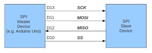
First on our list today is the use of multiple SPI devices on the single bus. We briefly touched on this in part one, by showing how multiple devices are wired, for example:


Notice how the slave devices share the clock, MOSI and MISO lines – however they both have their own chip select line back to the master device. At this point a limitation of the SPI bus becomes prevalent – for each slave device we need another digital pin to control chip select for that device. If you were looking to control many devices, it would be better to consider finding I2C solutions to the problem.
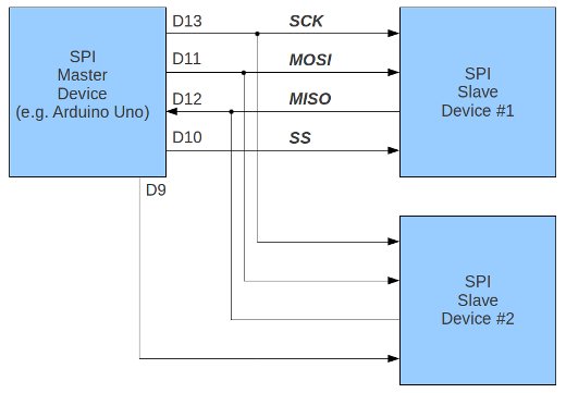
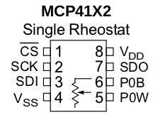
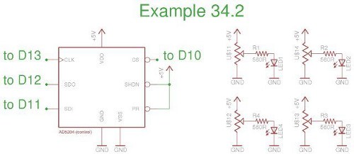
To implement multiple devices is very easy. Consider the example 34.1 from part one – we controlled a digital rheostat. Now we will repeat the example, but instead control four instead of one. For reference, here is the pinout diagram:


Doing so may sound complex, but it is not. We connect the SCK, MOSI and MISO pins together, then to Arduino pins D13, D11, D12 respectively. Each CS pin is wired to a separate Arduino digital pin. In our example rheostats 1 to 4 connect to D10 through to D7 respectively. To show the resistance is changing on each rheostat, there is an LED between pin 5 and GND and a 470 ohm resistor between 5V and pin 6. Next, here is the sketch:
/*
Multiple SPI bus device demo using four Microchip MCP4162s
*/

#include "SPI.h" // necessary library
int del=3; // used for various delays

int led1=10; // CS lines for each SPI device
int led2=9;
int led3=8;
int led4=7;

void setup()
{
  pinMode(led1, OUTPUT);
  pinMode(led2, OUTPUT);
  pinMode(led3, OUTPUT);
  pinMode(led4, OUTPUT);
  digitalWrite(led1, HIGH);
  digitalWrite(led2, HIGH);
  digitalWrite(led3, HIGH);
  digitalWrite(led4, HIGH);
  SPI.begin(); // wake up the SPI bus.
  SPI.setBitOrder(MSBFIRST);
  // our MCP4162s requires data to be sent MSB (most significant byte) first
}

void setValue(int l, int value)
// sends value 'value' to SPI device on CS digital out pin 'l'
{
  digitalWrite(l, LOW);
  SPI.transfer(0); // send command byte
  SPI.transfer(value); // send value (0~255)
  digitalWrite(l, HIGH);
}

void allOff()
// sets all pots to max resistance
{
     setValue(led1,255);
     setValue(led2,255);
     setValue(led3,255);
     setValue(led4,255);
}

void pulse(int l)
{
  allOff();
  for (int a=255; a>=0; --a)
  {
    setValue(l,a);
    delay(del);
  }
  for (int a=0; a<256; a++)
  {
    setValue(l,a);
    delay(del);
  }
}

void pulseAll()
{
  allOff();
  for (int a=255; a>=0; --a)
  {
    setValue(led1,a);
    setValue(led2,a);
    setValue(led3,a);
    setValue(led4,a);
    delay(del);
  }
  for (int a=0; a<256; a++)
  {
    setValue(led1,a);
    setValue(led2,a);
    setValue(led3,a);
    setValue(led4,a);
    delay(del);
  }
}

void loop()
{
  pulse(led1);
  pulse(led2);
  pulse(led3);
  pulse(led4);
  pulseAll();
}
Although the example sketch may be longer than necessary, it is quite simple. We have four SPI devices each controlling one LED, so to keep things easy to track we have defined led1~led4 to match the chip select digital out pins used for each SPI device.
Then see the first four lines in void setup(); these pins are set to output in order to function as required. Next – this is very important – we set the pins’ state to HIGH.
You must do this to every chip select line! Otherwise more than one CS pins may be initially low in some instances and cause the first data sent from MOSI to travel along to two or more SPI devices. With LEDs this may not be an issue, but for motor controllers … well it could be.
The other point of interest is the function
void setValue(int l, int value)
We pass the value for the SPI device we want to control, and the value to send to the device. The value for l is the chip select value for the SPI device to control, and ranges from 10~7 – or as defined earlier, led1~4. The rest of the sketch is involved in controlling the LED’s brightness by varying the resistance of the rheostats. Now to see example 36.1 in action via the following video clip:
Next on the agenda is a digital-to-analogue converter, to be referred to using the acronym DAC. What is a DAC? In simple terms, it accepts a numerical value between zero and a maximum value (digital) and outputs a voltage between the range of zero and a maximum relative to the input value (analogue).
One could consider this to be the opposite of the what we use the function analogRead(); for. For our example we will use a Microchip MCP4921 (data sheet.pdf):


(Please note that this is a beginners’ tutorial and is somewhat simplified). This DAC has a 12-bit resolution. This means that it can accept a decimal number between 0 and 4095 – in binary this is 0 to 1111 1111 1111 (see why it is called 12-bit) – and the outpout voltage is divided into 4096 steps. The output voltage for this particular DAC can fall between 0 and just under the supply voltage (5V). So for each increase of 1 in the decimal input value, the DAC will output around 1.221 millivolts.
It is also possible to reduce the size of the voltage output steps by using a lower reference voltage. Then the DAC will consider the reference voltage to be the maximum output with a value of 4095. So (for example) if the reference voltage was 2.5V, each increase of 1 in the decimal input value, the DAC will output around 0.6105 millivolts. The minimum reference voltage possible is 0.8V, which offers a step of 200 microvolts (uV).
The output of a DAC can be used for many things, such as a function generator or the playback of audio recorded in a digital form. For now we will examine how to use the hardware, and monitoring output on an oscilloscope. First we need the pinouts:


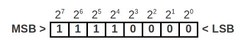
By now these sorts of diagrams shouldn’t present any problems. In this example, we keep pin 5 permanently set to GND; pin 6 is where you feed in the reference voltage – we will set this to +5V; AVss is GND; and Vouta is the output signal pin – where the magic comes from 🙂 The next thing to investigate is the MCP4921’s write command register:


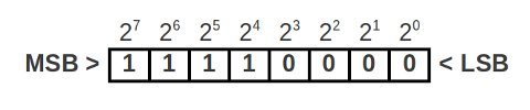
Bits 0 to 11 are the 12 bits of the output value; bit 15 is an output selector (unused on the MPC4921); bit 14 controls the input buffer; bit 13 controls an inbuilt output amplifier; and bit 12 can shutdown the DAC. Unlike previous devices, the input data is spread across two bytes (or a word of data).
Therefore a small amount of work needs to be done to format the data ready for the DAC. Let’s explain this through looking at the sketch for example 36.2 that follows. The purpose of the sketch is to go through all possible DAC values, from 0 to 4095, then back to 0 and so on.
First. note the variable outputvalue – it is a word, a 16-bit unsigned variable. This is perfect as we will be sending a word of data to the DAC. We put the increasing/decreasing value for a into outputValue. However as we can only send bytes of data at a time down the SPI bus, we will use the function highbyte() to separate the high side of the word (bits 15~8) into a byte variable called data.
We then use the bitwise AND and OR operators to set the parameter bits 15~12. Then this byte is sent to the SPI bus. Finally, the function lowbyte() is used to send the low side of the word (bits 7~0) into data and thence down the SPI bus as well.
Now for our demonstration sketch:
/*
SPI bus device demo using a Microchip MCP4921 DAC
 */

#include "SPI.h" // necessary library
int del=0; // used for various delays
word outputValue = 0; // a word is a 16-bit number
byte data = 0; // and a byte is an 8-bit number
void setup()
{
  //set pin(s) to input and output
  pinMode(10, OUTPUT);
  SPI.begin(); // wake up the SPI bus.
  SPI.setBitOrder(MSBFIRST);
}

void loop()
{
  for (int a=0; a<=4095; a++)
  {
    outputValue = a;
    digitalWrite(10, LOW);
    data = highByte(outputValue);
    data = 0b00001111 & data;
    data = 0b00110000 | data;
    SPI.transfer(data);
    data = lowByte(outputValue);
    SPI.transfer(data);
    digitalWrite(10, HIGH);
    delay(del);
  }
  delay(del+25);
  for (int a=4095; a>=0; --a)
  {
    outputValue = a;
    digitalWrite(10, LOW);
    data = highByte(outputValue);
    data = 0b00001111 & data;
    data = 0b00110000 | data;
    SPI.transfer(data);
    data = lowByte(outputValue);
    SPI.transfer(data);
    digitalWrite(10, HIGH);
    delay(del);
  }
  delay(del+25);
}
And a quick look at the DAC in action via an oscilloscope:
By now we have covered in detail how to send data to a device on the SPI bus. But how do we receive data from a device?
Doing so is quite simple, but some information is required about the particular device. For the rest of this chapter, we will use the Maxim DS3234 “extremely accurate” real-time clock. Please download the data sheet (.pdf) now, as it will be referred to many times.
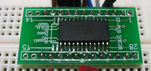
The DS3234 is not available in through-hole packaging, so we will be using one that comes pre-soldered onto a breakout board:


It only takes a few moments to solder in some header pins for breadboard use. The battery type is CR1220 (12 x 2.0mm, 3V); if you don’t have a battery you will need to short out the battery holder with some wire otherwise the IC will not work. Readers have reported that the IC doesn’t keep time if the USB and external power are both applied to the Arduino at the same time.
A device will have one or more registers where information is read from and written to. Look at page twelve of the DS3234 data sheet, there are twenty-three registers, each containing eight bits (one byte) of data.
Please take note that each register has a read and write address. An example – to retrieve the contents of the register at location 08h (alarm minutes) and place it into the byte data we need to do the following:
digitalWrite(10, LOW); // select the DS3234 that has its CS line on digital 10
SPI.transfer(0x08); // tell the DS3234 device we're requesting data from the register at 08h
data=SPI.transfer(0); // the DS3234 sends the data back and stores it in the byte data
digitalWrite(10, HIGH);  // deselect the DS3234 if finished with it
Don’t forget to take note of the function SPI.setBitOrder(MSBFIRST); in your sketch, as this also determines the bit order of the data coming from the device. To write data to a specific address is also quite simple, for example:
digitalWrite(10, LOW);
SPI.transfer(0x80); // tells the device which address to write to
SPI.transfer(b00001010);   // you can send any representation of a byte
digitalWrite(10, HIGH);
Up to this point, we have not concerned ourselves with what is called the SPI data mode. The mode determines how the SPI device interprets the ‘pulses’ of data going in and out of the device.
For a well-defined explanation, please read this article. With some devices (and in our forthcoming example) the data mode needs to be defined. So we use:
SPI.setDataMode(SPI_MODE1);
to set the data mode, within void(setup);. To determine a device’s data mode, as always – consult the data sheet. With our DS3234 example, the mode is mentioned on page 1 under Features List.
Finally, let’s delve a little deeper into SPI via the DS3234. The people at Sparkfun have already written a good demonstration sketch for the DS3234, so let’s have a look at that and deconstruct it a little to see what is going on. You can download the sketch below from here, then change the file extension from .c to .pde.
#include "SPI.h"
const int  cs=8; //chip select

void setup() {
  Serial.begin(9600);
  RTC_init();
  //day(1-31), month(1-12), year(0-99), hour(0-23), minute(0-59), second(0-59)
  SetTimeDate(11,12,13,14,15,16);
}

void loop() {
  Serial.println(ReadTimeDate());
  delay(1000);
}
//=====================================
int RTC_init(){
	  pinMode(cs,OUTPUT); // chip select
	  // start the SPI library:
	  SPI.begin();
	  SPI.setBitOrder(MSBFIRST);
	  SPI.setDataMode(SPI_MODE1); // both mode 1 & 3 should work
	  //set control register
	  digitalWrite(cs, LOW);
	  SPI.transfer(0x8E);
	  SPI.transfer(0x60); //60= disable Osciallator and Battery SQ wave @1hz, temp compensation, Alarms disabled
	  digitalWrite(cs, HIGH);
	  delay(10);
}
//=====================================
int SetTimeDate(int d, int mo, int y, int h, int mi, int s){
	int TimeDate [7]={s,mi,h,0,d,mo,y};
	for(int i=0; i<=6;i++){
		if(i==3)
			i++;
		int b= TimeDate[i]/10;
		int a= TimeDate[i]-b*10;
		if(i==2){
			if (b==2)
				b=B00000010;
			else if (b==1)
				b=B00000001;
		}
		TimeDate[i]= a+(b<<4);

		digitalWrite(cs, LOW);
		SPI.transfer(i+0x80);
		SPI.transfer(TimeDate[i]);
		digitalWrite(cs, HIGH);
  }
}
//=====================================
String ReadTimeDate(){
	String temp;
	int TimeDate [7]; //second,minute,hour,null,day,month,year
	for(int i=0; i<=6;i++){
		if(i==3)
			i++;
		digitalWrite(cs, LOW);
		SPI.transfer(i+0x00);
		unsigned int n = SPI.transfer(0x00);
		digitalWrite(cs, HIGH);
		int a=n & B00001111;
		if(i==2){
			int b=(n & B00110000)>>4; //24 hour mode
			if(b==B00000010)
				b=20;
			else if(b==B00000001)
				b=10;
			TimeDate[i]=a+b;
		}
		else if(i==4){
			int b=(n & B00110000)>>4;
			TimeDate[i]=a+b*10;
		}
		else if(i==5){
			int b=(n & B00010000)>>4;
			TimeDate[i]=a+b*10;
		}
		else if(i==6){
			int b=(n & B11110000)>>4;
			TimeDate[i]=a+b*10;
		}
		else{
			int b=(n & B01110000)>>4;
			TimeDate[i]=a+b*10;
			}
	}
	temp.concat(TimeDate[4]);
	temp.concat("/") ;
	temp.concat(TimeDate[5]);
	temp.concat("/") ;
	temp.concat(TimeDate[6]);
	temp.concat("     ") ;
	temp.concat(TimeDate[2]);
	temp.concat(":") ;
	temp.concat(TimeDate[1]);
	temp.concat(":") ;
	temp.concat(TimeDate[0]);
  return(temp);
}
Don’t let the use of custom functions and loops put you off, they are there to save time. Looking in the function SetTimeDate();, you can see that the data is written to the registers 80h through to 86h (skipping 83h – day of week) in the way as described earlier (set CS low, send out address to write to, send out data, set CS high).
You will also notice some bitwise arithmetic going on as well. This is done to convert data between binary-coded decimal and decimal numbers.
Why? Go back to page twelve of the DS3234 data sheet and look at (e.g.) register 00h/80h – seconds. The bits 7~4 are used to represent the ‘tens’ column of the value, and bits 3~0 represent the ‘ones’ column of the value.
So some bit shifting is necessary to isolate the digit for each column in order to convert the data to decimal. Finally here is another example of reading the time data from the DS3234:
/*
SPI bus device demo using a Maxim IC DS3234 Accurate RTC
 */
#include "SPI.h" // necessary library
// store hours, minutes, seconds, day of month, month, year
byte h,m,s,d,mo,y;
void setup()
{
 pinMode(10, OUTPUT);
 SPI.begin(); // wake up the SPI bus.
 SPI.setBitOrder(MSBFIRST);
 SPI.setDataMode(SPI_MODE1);
 digitalWrite(10, LOW);

 SPI.transfer(0x8E); // write to control register 8Eh (page 14 data sheet)
 SPI.transfer(0x60); // oscillator on, 1Hz, alarms off (b01100000)
 digitalWrite(10, HIGH);
 Serial.begin(9600);
}

void readDS3234()
{
 byte data=0;
 int a,b=0;
 digitalWrite(10, LOW);

 // get seconds
 SPI.transfer(0x00); // get seconds data from register 00h
 data=SPI.transfer(0x00);
 a = data & B00001111; // isolates 1's column
 b = (data & B01110000)>>4; // isolates 10's digit
 s=(b*10)+a; // calculate seconds!

 // get minutes
 SPI.transfer(0x01); // get minutes data from register 00h
 data=SPI.transfer(0x00);
 a = data & B00001111; // isolates 1's column
 b = (data & B01110000)>>4; // isolates 10's digit
 m=(b*10)+a; // calculate minutes!

 // get hours
 SPI.transfer(0x02); // get minutes data from register 00h
 data=SPI.transfer(0x00);
 a = data & B00001111; // isolates 1's column
 b = (data & B00110000)>>4; // isolate upper nibble
 if (b==B00000010) // 24 hr time
 {
 b=20;
 } else
 if (b==B00000001) // 12 hr time
 {
 b=10;
 }
 h = a + b; // calculate hours

 digitalWrite(10, HIGH);
}
void loop()
{
 readDS3234();
 Serial.print(h, DEC);
 Serial.print(":");
 if (m<10)
 {
 Serial.print("0");
 }
 Serial.print(m, DEC);
 Serial.print(":");
 if (s<10)
 {
 Serial.print("0");
 }
 Serial.print(s, DEC);
 Serial.println();
 delay(500);
}
So there you have it – more about the world of the SPI bus and how to control the devices within.
This post brought to you by pmdway.com – everything for makers and electronics enthusiasts, with free delivery worldwide.
To keep up to date with new posts at tronixstuff.com, please subscribe to the mailing list in the box on the right, or follow us on twitter @tronixstuff.


You must be logged in to post a comment.